Interfacing the MAX195 ADC to

Interfacing the MAX195 ADC to,第1张

Abstract: ApplicaTIon note for interfacing the MAX195 and MAX194 analog-to-digital converters (ADCs) to the TMS320C3X evaluaTIon module. Example demo code is given. The demo software configures the TMS320C30 so that FSR1 and DR1 are inputs and CLKR1 and XF1 are outputs. To read the MAX194/MAX195, the software briefly drives the XF1 output low. The demo software polls the serial receiver unTIl a complete frame has been received. Because this is just an interface demo, the software simply writes the received data word to the EVM host data port.

OverviewThe MAX195 16-bit ADC can be interfaced to Texas Instruments' TMS320C30 DSP by means of its serial interface. The interface uses four wires plus ground. This applicaTIon note explains how to interface the MAX194/MAX195 Evaluation Kit to the TMS320C3X Evaluation Module.

The example program was assembled using the TMS320C3X/4X COFF Assembler Version 4.50 and the TMS320C3X/4F COFF Linker Version 4.50 (copyright 1987 through 1992 by Texas Instruments Incorporated).

Interfacing the MAX194/MAX195 EVKIT to the TMS320C3X EVMMaxim's MAX194/MAX195 Evaluation Kit can be interfaced to Texas Instruments' TMS320C3X Evaluation Module as follows:
  1. Set the MAX194/MAX195 EVKIT jumpers according to Table 1.
  2. Solder a 2-x-5-pin berg strip into MAX194/MAX195 EVKIT area J3. The PC board is already wired as shown in Table 2.
  3. Connect a +5V power supply to the MAX194/MAX195 EVKIT.
  4. Connect a 10-pin ribbon cable between the TMS320C3X EVM and the MAX194/MAX195 EVKIT.
  5. Run the demo software.
Table 1. Jumper Settings Jumper Position Function JU1
Closed
Connects the MAX195 SCLK to ground
JU3
EXT
TMS320 CLKR1 drives the MAX195 conversion clock.
JU4
CS = GND
Connects the MAX195 Active-Low CS to ground
JU5
QSPI
TMS320 XF1 drives the MAX195 CONV.
JU6
Open
MAX195 reset/calibration command
JU7
UNI or OPEN
Selects unipolar or bipolar transfer function

Table 2. Ribbon-Cable Signals
Pin MAX195 TMS320 Pin MAX195 TMS320 1
DGND
GND
2
Active-Low EOC
FSR1
3
Not used
4
DOUT
DR1
5
Not used
6
Not used
7
Not used
8
Active-Low CONV
XF1
9
CONCLK
CLKR1
10
DGND
GND
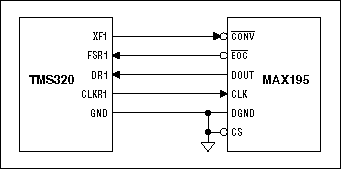
How It WorksThe demo software (see the program-code listing that follows) configures the TMS320C30 so that FSR1 and DR1 are inputs and CLKR1 and XF1 are outputs. The software uses the XF1 output to initiate a conversion. The XF1 pulse drives the MAX194/MAX195 conversion start input. The CLKR1 output provides the conversion clock to the MAX194/MAX195. Data output from the MAX194/MAX195 is received on the DR1 input. The FSR1 Frame Start signal is driven by the MAX194/MAX195 EOC (End of Conversion) signal, which marks the beginning of the serial frame.

To read the MAX194/MAX195, the software briefly drives the XF1 output low. The demo software polls the serial receiver until a complete frame has been received. Because this is just an interface demo, the software simply writes the received data word to the EVM host data port. TMS320C3x/4x COFF Assembler, Version 4.50 Copyright (c) 1987-1992, Texas Instruments Incorporated TMS320C30 Serial Port Initialization
Project: MAX195 EVKIT Interface to TMS320C3X EVM
Project file = MAX195I

Filename = MAX195I.ASM
Command file = MAX195I.CMD

Compile with the following commands:

   asm30 MAX195I -l
   lnk30 MAX195I.CMD

Pin Assignments:

Interfacing the MAX195 ADC to,第2张

Note: jumper JU8 must be OPEN
and CS must be tied to GND

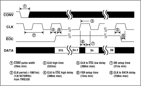
Timing Diagram:
Interfacing the MAX195 ADC to,第3张

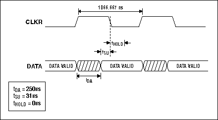
Fastest Clock 1MHz = (1 / 1000 nsec)
Minimum Receiver Timer Period = 4H

Receive Timer Period = 4 = 0.9375MHz
(System clock frequency = 30MHz)

Word diagram:

Interfacing the MAX195 ADC to,第4张

Interfacing the MAX195 ADC to,Figure 1. Schematic.,第5张
Figure 1. Schematic.

Interfacing the MAX195 ADC to,Figure 2. Timing.,第6张
Figure 2. Timing


欢迎分享,转载请注明来源:内存溢出

原文地址: http://outofmemory.cn/dianzi/2547304.html

(0)
打赏 微信扫一扫 微信扫一扫 支付宝扫一扫 支付宝扫一扫
上一篇 2022-08-05
下一篇 2022-08-05

发表评论

登录后才能评论

评论列表(0条)

保存