
latTIce公司的MachXO3LF-9400C是支持大多数先进可编程桥接和IO扩展的超低密度PLD系列,密度范围从640查找表(LUT)到9400 LUT.此外,低成本可编逻辑器件具有嵌入区块RAM(EBR),分布式RAM,锁相环(PLL),支持用户闪存(UFM)。采用65nm非易失低功耗工艺,特别适合用在低成本量大的系统应用如消费类电子,计算与存储,无线通信,工业控制系统和汽车系统。本文介绍了MachXO3LF-9400C主要特性和结构图,以及MachXO3-9400™开发板主要特性,框图,电路图和材料清单。
These features help manage staTIc and dynamic power consumpTIon resulTIng in low static power for all members of the family. The MachXO3L/LF devices are available in two versions C and E with two speed grades: -5 and -6, with -6 being the fastest. C devices have an internal linear voltage regulator which supports external VCC supply voltages of 3.3 V or 2.5 V. E devices only accept 1.2 V as the external VCC supply voltage. With the exception of power supply voltage both C and E are functionally compatible with each other. The MachXO3L/LF PLDs are available in a broad range of advanced halogen-free packages ranging from the space saving 2.5 x 2.5 mm WLCSP to the 19 x 19 mm caBGA. MachXO3L/LF devices support density migration within the same package. Table 1-1 shows the LUT densities, package and I/O options, along with other key parameters. The MachXO3L/LF devices offer enhanced I/O features such as drive strength control, slew rate control, PCI com-patibility, bus-keeper latches, pull-up resistors, pull-down resistors, open drain outputs and hot socketing. Pull-up, pull-down and bus-keeper features are controllable on a “per-pin” basis. A user-programmable internal oscillator is included in MachXO3L/LF devices. The clock output from this oscillator may be divided by the timer/counter for use as clock input in functions such as LED control, key-board scanner and similar state machines. The MachXO3L/LF devices also provide flexible, reliable and secure configuration from on-chip NVCM/Flash. These devices can also configure themselves from external SPI Flash or be configured by an external master through the JTAG test access port or through the I2C port. Additionally, MachXO3L/LF devices support dual-boot capability (using external Flash memory) and remote field upgrade (TransFR) capability. Lattice provides a variety of design tools that allow complex designs to be efficiently implemented using the MachXO3L/LF family of devices. Popular logic synthesis tools provide synthesis library support for MachXO3L/LF. Lattice design tools use the synthesis tool output along with the user-specified preferences and constraints to place and route the design in the MachXO3L/LF device. These tools extract the timing from the routing and back-anno-tate it into the design for timing verification. Lattice provides many pre-engineered IP (Intellectual Property) LatticeCORE™ modules, including a number of reference designs licensed free of charge, optimized for the MachXO3L/LF PLD family. By using these configurable soft core IP cores as standardized blocks, users are free to concentrate on the unique aspects of their design, increasing their productivity.
MachXO3LF-9400C主要特性:
Solutions
• Smallest footprint, lowest power, high data throughput bridging solutions for mobile applications
• Optimized footprint, logic density, IO count, IO performance devices for IO management and logic applications
•High IO/logic, lowest cost/IO, high IO devices for IO expansion applications
Flexible Architecture
• Logic Density ranging from 640 to 9.4K LUT4
•High IO to LUT ratio with up to 384 IO pins
Advanced Packaging
• 0.4 mm pitch: 1K to 4K densities in very small footprint WLCSP (2.5 mm x 2.5 mm to 3.8 mm x 3.8 mm) with 28 to 63 IOs
• 0.5 mm pitch: 640 to 9.4K LUT densities in 6 mm x 6 mm to 10 mm x 10 mm BGA packages with up to 281 IOs
•0.8 mm pitch: 1K to 9.4K densities with up to 384 IOs in BGA packages
Pre-Engineered Source Synchronous I/O
• DDR registers in I/O cells
• Dedicated gearing logic
• 7:1 Gearing for Display I/Os
•Generic DDR, DDRx2, DDRx4
High Performance, Flexible I/O Buffer
• Programmable sysIOTM buffer supports wide range of interfaces:
— LVCMOS 3.3/2.5/1.8/1.5/1.2
— LVTTL
— LVDS, Bus-LVDS, MLVDS, LVPECL
— MIPI D-PHY Emulated
— Schmitt trigger inputs, up to 0.5 V hysteresis
•Programmable pull-up or pull-down mode
• Ideal for IO bridging applications
• I/Os support hot socketing
• On-chip differential termination
Flexible On-Chip Clocking
• Eight primary clocks
• Up to two edge clocks for high-speed I/O inter-faces (top and bottom sides only)
• Up to two analog PLLs per device with frac-tional-n frequency synthesis
— Wide input frequency range (7 MHz to 400 MHz)
Non-volatile, Multi-time Programmable
• Instant-on
— Powers up in microseconds
• Optional dual boot with external SPI memory
• Single-chip, secure solution
• Programmable through JTAG, SPI or I2C
• MachXO3L includes multi-time programmable NVCM
• MachXO3LF infinitely reconfigurable Flash
— Supports background programming of non-volatile memory
TransFR Reconfiguration
•In-field logic update while IO holds the system state
Enhanced System Level Support
• On-chip hardened functions: SPI, I2C, timer/ counter
• On-chip oscillator with 5.5% accuracy
• Unique TraceID for system tracking
• Single power supply with extended operating range
• IEEE Standard 1149.1 boundary scan
•IEEE 1532 compliant in-system programming
MachXO3LF-9400C应用:
• Consumer Electronics
• Compute and Storage
• Wireless Communications
• Industrial Control Systems
•Automotive System
Low Cost Migration Path
• Migration from the Flash based MachXO3LF to the NVCM based MachXO3L
• Pin compatible and equivalent timing
The MachXO3L/LF family architecture contains an array of logic blocks surrounded by Programmable I/O (PIO)。 All logic density devices in this family have sysCLOCK™ PLLs and blocks of sysMEM Embedded Block RAM (EBRs)。
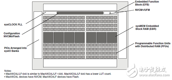
图1.MachXO3L/LF-1300器件结构图
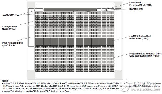
图2.MachXO3L/LF-4300器件结构图
MachXO3-9400™开发板
The Lattice Semiconductor MachXO3-9400™ Development Board allows designers to investigate and experiment with the features of the MachXO3 complex programmable logic device (CPLD) and the L-ASC10 (L-Analog Sense and Control 10 rails) hardware management expander. The features of the MachXO3-9400 Development Board can assist engineers with the rapid prototyping and testing of their specific designs.The MachXO3-9400 Development Board is part of the MachXO3-9400 Development Kit, which includes the following:
MachXO3-9400 Development Board pre-loaded with the demo design
Mini USB cable
QuickStart Guide
Along with the MachXO3LF-9400 CPLD, the MachXO3-9400 Development Board also features an L-ASC10 device to enable designers to easily evaluate hardware management design and expand the usability of the MachXO3LF-9400 with Arduino, Raspberry, FX12, Versa and Aardvark headers.
MachXO3-9400™开发板主要特性:
LCMXO3LF-9400C CPLD demonstration with L-ASC10 for simple hardware management including voltage, current and temperature monitoring
General Purpose Input/Output (GPIO) interface with Arduino and Raspberry Pi boards
USB-B connection for device programming and Inter-Integrated Circuit (I2C) utility
On-board Boot Flash–16 Mbit Serial Peripheral Interface (SPI) Flash, with Quad read feature for user’s application
4-position DIP Switches, 4 push buttons and 16 LEDs for demo purposes
Diamond® programming support
Multiple reference clock sources
Two Hirose FX12-40 header positions (DNI)
Aardvark header (DNI)
图3.MachXO3-9400™开发板顶视图
图4.MachXO3-9400™开发板底视图
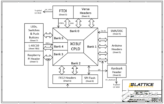
图5.MachXO3-9400™开发板框图
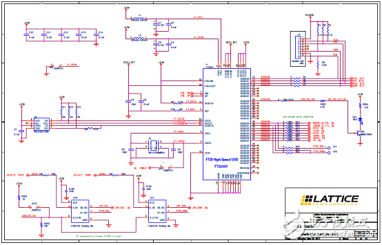
图6.MachXO3-9400™开发板电路图(1):USB到JTAG I/F
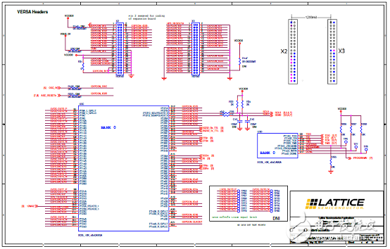
图7.MachXO3-9400™开发板电路图(2):VERSA插座(BANK0)
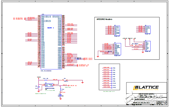
图8.MachXO3-9400™开发板电路图(3):Arduino插座(BANK1)
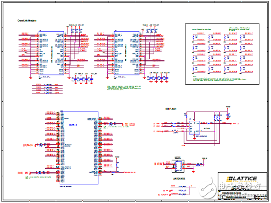
图9.MachXO3-9400™开发板电路图(4):CrossLink插座(BANK2)
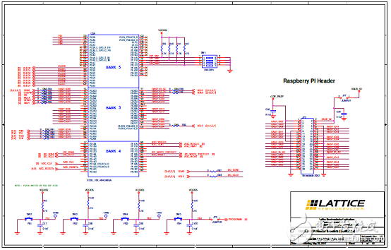
图10.MachXO3-9400™开发板电路图(5):Raspberry Pi插座和其它(BANK3,BANK4,BANK5)
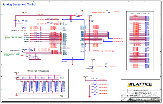
图11.MachXO3-9400™开发板电路图(6):模拟检测和控制
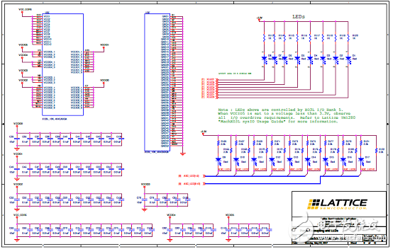
图12.MachXO3-9400™开发板电路图(7):电源去耦和LED
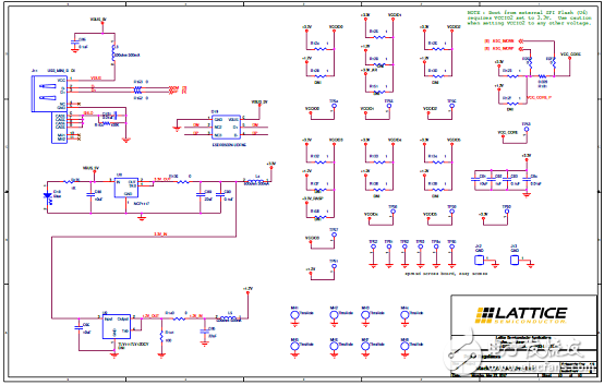
图13.MachXO3-9400™开发板电路图(8):电源稳压器
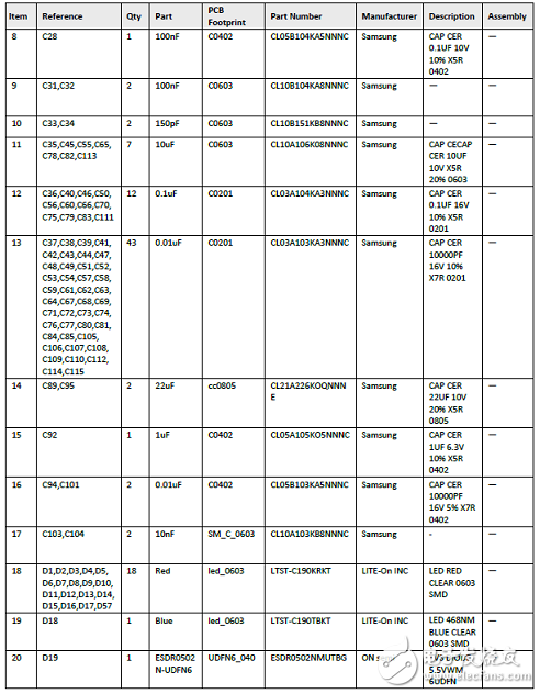
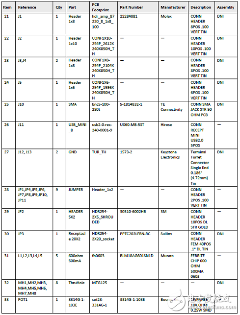
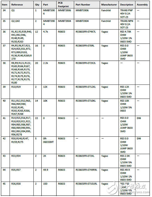
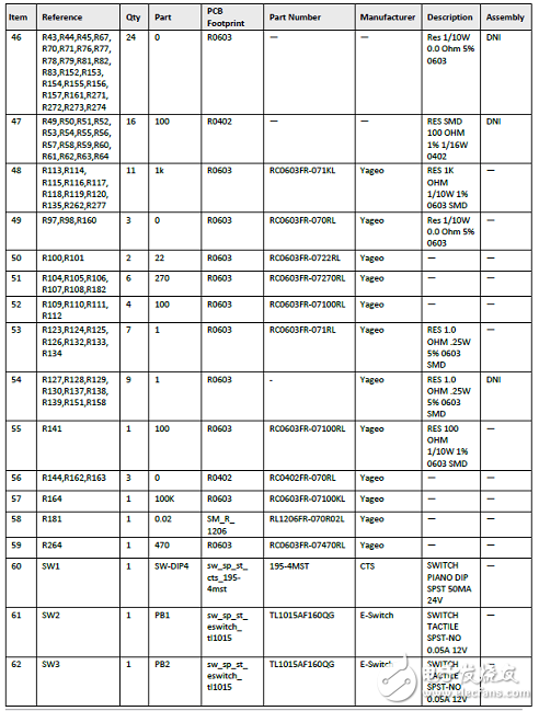
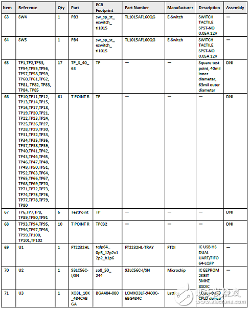
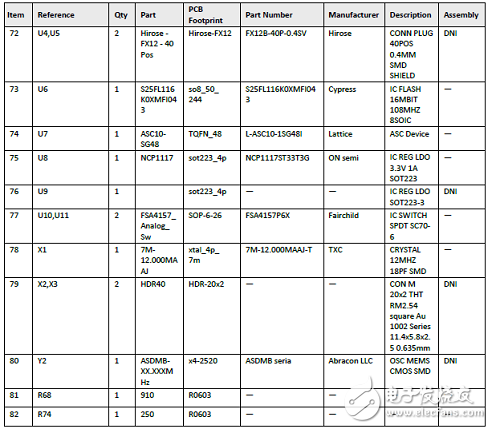
MachXO3-9400™开发板材料清单:
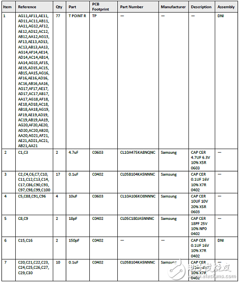
欢迎分享,转载请注明来源:内存溢出

 微信扫一扫
微信扫一扫
 支付宝扫一扫
评论列表(0条)