
S6BP201A is a 1-Ch Buck-boost DC/DC converter IC with four built-in switching FETs. This IC is able to supply up to 1.0A of loadcurrent within the very wide range from 2.5V to 42V in the input voltage. This IC has an operaTIon mode that is automaTIcally changedto PFM operaTIon during low load, which can achieve super-high efficiency with a very low quiescent current 20 μA. It is possible toprovide stable output voltage from an automoTIve cold cranking and load dump, up to 42V, conditions within 1 ms transition time. As aresult, this IC is suitable for power supply solutions of automotive and Industrial applications. This IC has the SYNC function, which iscapable of selecting the SYNC_IN that is able to inputs an external clock signal. When an external clock signal in the range from 200kHz to 400 kHz is inputted, the FETs perform the switching operation with synchronizing signal from an external clock. When anexternal clock signal is not inputted, the FETs perform the switching operation from an internal clock. The internal clock signal in therange from 200 kHz to 2.1 MHz can be set by an external resistor. Since external voltage setting resistors and phase compensationcapacitors are not required with this IC, it can reduce the number of parts and a part mounting area. This IC has five protectionfunctions, input under voltage lockout (input UVLO), output under voltage protection (output UVP), output over voltage protection(output OVP), output over current protection (output OCP), and thermal shutdown (TSD)。 Moreover, this IC has the power good (PG)function that indicates the state of the output voltage (VOUT pin)。 When the output voltage reaches the PG voltage, the PG signal isoutputted. The VOUT output voltage of this product is selectable from the product lineup.
S6BP201A主要特性:
Wide input voltage range: 2.5V to 42V
Selectable output voltage (factory settable):
5.000V/5.050V/5.075V/5.100V/5.125V/5.150V/5.200V
Wide operating frequency range: 200 kHz to 2.1 MHz
External synchronized clock range: 200 kHz to 400 kHz
SYNC function
SYNC_IN: External clock input(Unless inputting clock, this IC operates by internal clock)
Super-high efficiency by PFM operation(When setting MODE pin to a low level)
Automatic PWM/PFM switching operation and fixed PWMoperation are selectable by MODE pin
Built-in switching FET
Synchronous current mode architecture
Shutdown current: Lower than 1 μA
Quiescent current: 20 μA
Power Good Monitor
Output voltage monitoring by window comparator
Power-on reset time: 14 ms
Soft start time without load dependence : 0.9 ms(When switching frequency =2.1 MHz)
Enhanced protection functions
Input under voltage lockout
Output under voltage protection: 95.5%
Output over voltage protection: 104.5%
Output over current protection
Thermal shutdown
Small ETSSOP16 package (exposed PAD): 5 mm × 6.4 mm
AEC-Q100 compliant (Grade-1)
S6BP201A应用:
Body Control Module (BCM)
Gateway module
Automotive applications
Industrial applications
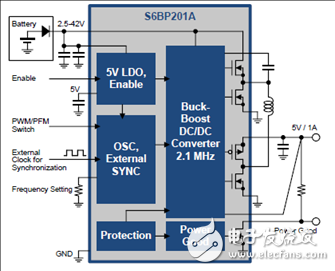
图1. S6BP201A框图
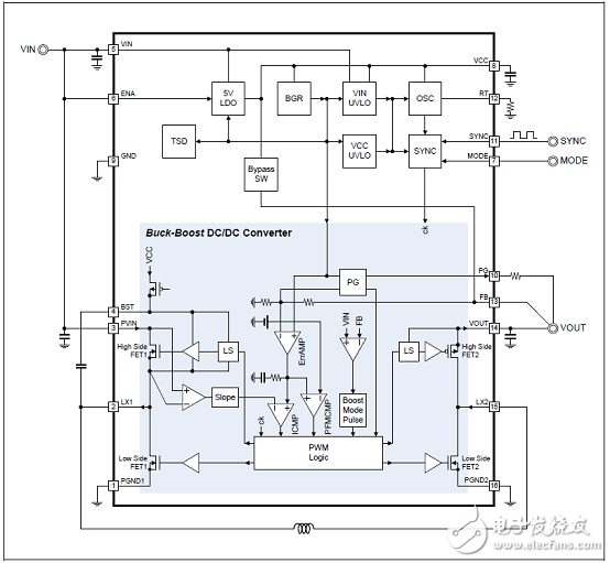
图2. S6BP201A架构框图
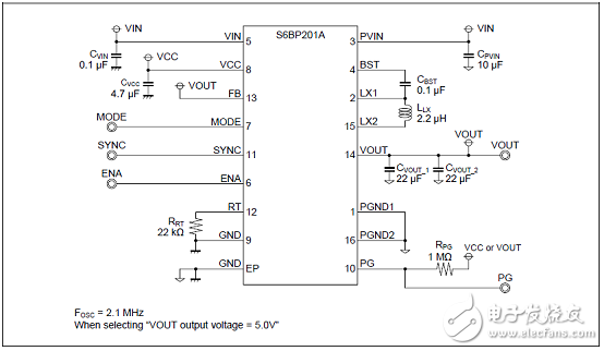
图3. S6BP201A应用案例电路图
应用案例电路元件列表:

评估板S6SBP201A1AVA1001,S6SBP202A1FVA1001和S6SBP203A8FVA1001
S6SBP201A1AVA1001, S6SBP202A1FVA1001 and S6SBP203A8FVA1001 are the evaluation kit forprimary power block of automotive.
These boards implement power management IC S6BP201A, S6BP202A, S6BP203A each.
It is necessary to prepare DC power supply.
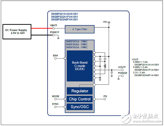
图4.评估板S6SBP201A1AVA1001,S6SBP202A1FVA1001和S6SBP203A8FVA1001框图
评估板S6SBP201A1AVA1001,S6SBP202A1FVA1001和S6SBP203A8FVA1001指标:

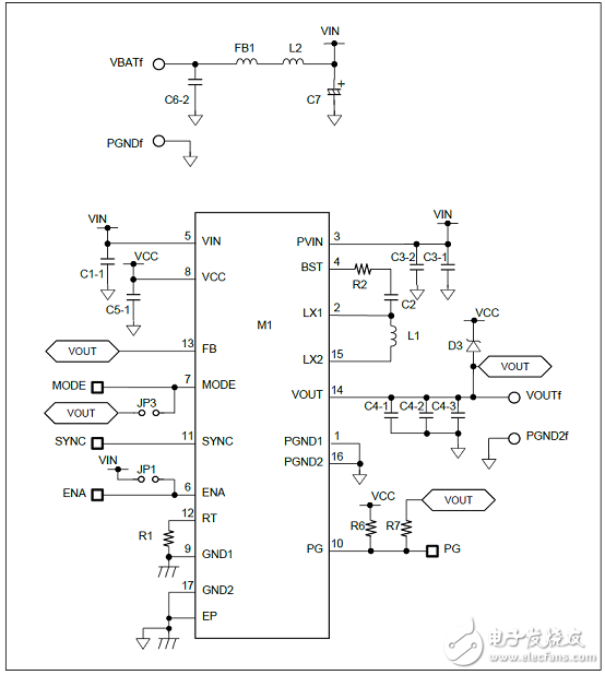
图5.评估板电路图
评估板S6SBP201A1AVA1001,S6SBP202A1FVA1001和S6SBP203A8FVA1001材料清单:
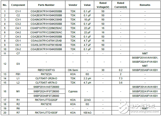
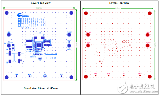
图6.评估板元件布局图

图7.评估板线布局图
欢迎分享,转载请注明来源:内存溢出

 微信扫一扫
微信扫一扫
 支付宝扫一扫
评论列表(0条)