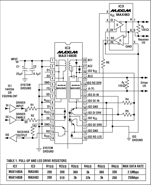
The simple RS-485 circuit of Figure 1 provides full-duplex communicaTIons (simultaneous transmission and recepTIon) with only two essential packages (IC2 and IC3). Its balanced and differential data lines are necessary for high-noise environments or for long-distance transmission between a computer and its peripherals. Such transmissions are difficult, if not impossible, with the single-ended circuitry of an RS-232 transceiver.
The RS-485 standard allows for bidirectional, multi-point, party-line communications, with data rates to 10M bits/second (10Mbps) and line lengths to 1200 meters. Differential transmission provides noise immunity. The circuit shown features controlled-slew-rate drivers that minimize EMI and the reflections caused by improperly terminated cables. It also enables error-free transmissions to 250kbps. To achieve data rates to 2.5Mbps, substitute a full-slew-rate MAX1480A for IC2, a MAX485 for IC3, and R2—R5 values per Table 1.

Figure 1. IC2 and IC3 provide full-duplex data communications for cable lengths as long as 1200 meters.
IC2 is a complete half-duplex interface that includes transceivers, optocouplers, a power driver, and a transformer. The optocouplers transmit digital signals across the internal isolation barrier, and the center-tapped transformer transmits power across the barrier from its logic (non-isolated) side to its isolated side.
IC3, powered by the isolated VCC, upgrades the half-duplex operation of IC2 to full duplex using IC2's own dedicated optocouplers. Pin 3 must be tied low to disable IC3's driver, and pin 4 should be left floating. The driver outputs for IC2 and IC3 exhibit high impedance when active-low DE is low; bringing active-low DE high enables the outputs to function as line drivers.
The isolation barrier in IC2 typically withstands 1600Vrms for one minute or 2000Vrms for one second. Any TTL/CMOS-logic family can drive the IC2 digital inputs through a series resistor. With resistive pull-ups, the receiver outputs can drive any such logic as well. IC2's isolated outputs meet all RS-485 specifications.
欢迎分享,转载请注明来源:内存溢出

 微信扫一扫
微信扫一扫
 支付宝扫一扫
评论列表(0条)