Introduction When developing products, EVKits (evaluation kits) are often used for evaluation and prototype development. Later, the EVKit board is replaced with the application's PCB (printed circuit board). For the MAX1452 and MAX1455, this requires proper interconnection between the application PCB and the KEY.
This application note describes how to make this change. It suggests a circuit diagram that can provide full operation of the signal conditioning device in digital and analog mode. This application note assumes that the serial interface board (KEY) and the communication software library (Serial.dll) that are supplied as part of the EVKIT package will be utilized to develop higher level routines to communicate with the compensation system. The KEY and the Serial.dll library are supplied as part of the MAX1452/55EVKITs and they are explained in detail in the MAX1452 and MAX1455 User Manuals.

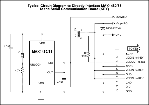
Figure 1. Descriptions The MAX1452 and MAX1455 signal conditioning products provide for digital conditioning (trimming) and analog amplification of the raw output of various sensors. Maxim has developed evaluation kits (EVKITs) to facilitate product evaluation and to reduce the time to market of the MAX1452/MAX1455 base products. The EVKIT package includes evaluation board, serial interface board, compensation software, control software, and serial communication software library (Serial.dll). As the user makes progress in product evaluation, the EVKIT board should be replaced with the application PCB and that requires proper interconnection between the application PCB and the KEY.
A typical circuit diagram to interface the MAX1452/MAX1455 products to the serial interface board is shown. Five pins (VDD, VSS, OUT, DIO, UNLOCK) from the MAX1452/MAX1455 products must be made accessible to operate the chip in both digital and analog modes. For analog operation of the product, only three lines are required, VDD, VSS, and OUT. The DIO and UNLOCK pins are needed, in addition to the other 3 pins, for digital communication only.
The supply voltage to the chip, VDD, must be selected form the VDDOUT, pin-3, of the KEY or directly from the Vsup line. In digital mode, the VDD pin must be supplied through the KEY. In digital mode, the communication software will turn the VDD line on-and-off as needed for initialization and synchronization of the digital communication with the device. In analog mode, the VDD is directly supplied from the Vsup line. Voltage source for the VDD pin is selected based on the setting of the J2 pins.
In this circuit, the OUT and DIO pins are permanently shorted together, OUT/DIO line. In digital mode, both OUT and DIO pins are high impedance unless the OUT pin is actually reporting the output voltage or the DIO pin is communicating with the controller as a digital output line. In analog mode, the DIO pin is high impedance at all time and the OUT pin is continuously reporting the module's output voltage.
The UNLOCK pin must be shorted to the VDD pin only in digital mode of operation. In the circuit presented here, this is accomplished by insertion of jumper J1.
Functions of the two jumpers is summarized below:
In a fully automated system, J1 and J2 jumpers should be replaced with software controlled switches as part of the test system.
The 10Ω, current limiting, resistor, on pin-3 of J2, is intended to prevent excessive current from/to the KEY. This resistor is not required if VDD pin is supplied directly from the Vsup line. Two 0.1uf capacitors are included in the circuit to reduce electrical noise on the VDD pin and the OUT pin. A Zener diode, BZX84C5V6, 5.6V, is added between the Vsup and the GND to protect against reverse voltage connection. Additional application specific components, if any, may be required that are not referenced in this application note. References
- MAX1452 Data Sheet.
- MAX1452 User Manual (includes MAX1452EVKIT manual).
- MAX1455 Data Sheet.
- MAX1455 User Manual (includes MAX1455EVKIT manual).
欢迎分享,转载请注明来源:内存溢出

 微信扫一扫
微信扫一扫
 支付宝扫一扫
评论列表(0条)