Reference Design of a 1-Wire BidirecTIonal Voltage-Level Translator for 1.8V to 5V
Abstract: Designers need open-drain logic to run at 1.8V at the 1-Wire master IO. Most 1-Wire slave devices cannot run at 1.8V. This applicaTIon note presents an RD (reference design) of a circuit that translates from a 1.8V 1-Wire master to a 5V 1-Wire slave device. The RD is used for driving typical 1-Wire slave devices. The MAX3394E voltage-level translator is featured in the design.
Today designers need open-drain logic to run at 1.8V at the 1-Wire master IO. While most 1-Wire slave devices can run safely at 5V, most of those same devices cannot run at 1.8V. A bidirectional voltage-level translator circuit is needed to overcome this limitation. This RD (reference design) features the Maxim® MAX3394E, which is a bidirectional voltage-level translator for these applications.
Voltage-Level Translator
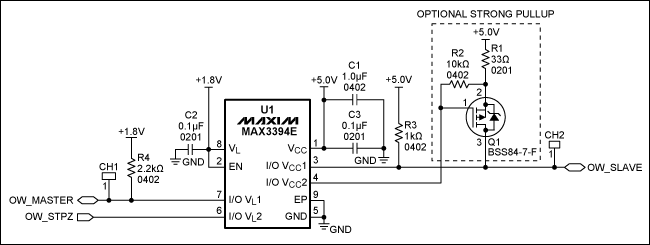
Application CircuitThe circuit in Figure 1 shows the MAX3394E used to perform bidirectional 1.8V to 5V voltage-level translation in an open-drain system.

Figure 1. Schematic of 1-Wire bidirectional voltage level translation from 1.8V to 5V. Note that the pins I/O VL and I/O VCC have a typical 10kΩ internal pullup.
The BOM (bill of materials) for this reference design is given in Table 1.
Table 1. Bill of Materials
Waveform Measurements/Test ResultsThe test results in Figures 2 through 5 were generated from the board built for evaluating the circuit.
Setup:
- VL = 1.8V
- VCC = 5.0V
- CH1: 1-Wire master (OW_MASTER)
- CH2: DS1920 (OW_SLAVE)
- OW_SLAVE wire length: 2.4m, max.
- Test results did not include the optional strong pullup circuitry in Figure 1.
- Room temperature measurements only
Figure 2. The scope plot of a 1-Wire Reset shows the performance of the MAX3394E with presence pulse amplitude of no more than 250mV, lower than a typical 1-Wire master VIL maximum of 0.4V.
Figure 3. The scope plot of a 1-Wire Write, one timeslot with a clean tLOW1 < 15µs.
Figure 4. The scope plot of a 1-Wire Write, zero timeslot with 60µs < tLOW0 < 120µs.
Figure 5. The scope plot of a 1-Wire Read, zero timeslot with an active 1-Wire slave open-drain return and lower than a typical 1-Wire master VIL maximum of 0.4V.
ConclusionThis RD for 1.8V to 5V 1-Wire bidirectional logic-level translation drives typical 1-Wire slave devices. The design was built and then tested. The circuit schematic, BOM, and typical waveforms have been presented.
欢迎分享,转载请注明来源:内存溢出

 微信扫一扫
微信扫一扫
 支付宝扫一扫
评论列表(0条)