
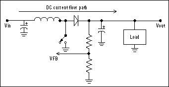
Figure 1. The problem of a direct path for current flow from source to load is intrinsic to the boost-converter topology.
Both problems are neatly solved for the relatively low output-current applications (<5A) that employ monolithic current-mode controllers and high-side current sensing. These circuits replace the catch diode with a synchronous switching transistor that can be disabled by shutdown or removal of input power. Disabling this internal transistor or turning it off during shutdown removes the path for DC current flow. The load then sees a requisite high-impedance disconnect. When not in shutdown, the circuit's cycle-by-cycle current-sensing mechanism (using an internal, high-side, current-sense resistor) protects against catastrophic meltdown from internal current overloads. Finally, thermal-overload protection provides a safe area of operation (SAO).
For applications with higher output current, in which pricing makes synchronous switching impractical for monolithic devices, the load-disconnect function requires a high-side switch external to the controller die. A discrete current-mode topology using a high-side current-sense resistor and a synchronous switching transistor is possible, but that approach suffers from PC-board parasitics and layout dependencies, especially at high switching frequencies. The result is a relatively complex design, particularly when system constraints mandate a low input voltage (<3.6V).
A synchronous, high-side external switch becomes feasible at higher levels of peak inductor current (>5A), but cost and complexity override heat and efficiency considerations at the more moderate levels of inductor current (~1.5A to 5A) discussed in this article. A simple catch diode is again the most desirable solution. The challenge is to achieve the desired load disconnect while retaining use of the humble catch diode and the unadorned boost topology.
A simple and smart solution is presented in Figure 2, where a MAX668 controller illustrates the demanding task of boosting from low input voltages. This current-mode boost controller drives a logic-level n-channel enhancement-mode MOSFET (configured on the low side) in series with a low-side current-sense resistor; neither is shown in Figure 2. Instead, this circuitry and the MAX668 are represented as a block to avoid cluttering the load connect/disconnect function. The high-side switch is a Schottky catch diode chosen for its low forward-voltage drop (now standard). The simple boost topology remains intact. This application boosts 3.3V to 5V and delivers load currents to 3A. The MAX668 boosts only from 3V or higher, but the MAX669 can accept inputs as low as 1.8V.
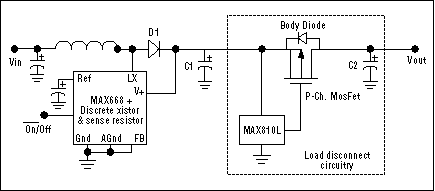
Figure 2. This boost converter with load disconnect illustrates the minimum-cost configuration.
The key element in implementing a smart load disconnect is the p-channel enhancement-mode MOSFET Q1. As shown, the system can enable this boost circuit (active-low ON ) or shut it down (OFF). D1 conducts during shutdown, producing 3.3V minus one diode drop at the MAX810L supply terminal. (This tiny power-on-reset device has a SOT23-3 package, draws about 24µA quiescent current, and guarantees operation at 1V.) In this case the MAX810L output is high, because its nominal reset threshold is 4.65V, which forces Q1 off and disconnects the load from the main supply.
The MAX668 feedback resistors are set to produce a 5V output when that device exits shutdown. When the rising output exceeds the MAX810L input threshold, an internal one-shot turns on for approximately 240msec. After this timeout period, the MAX810 output goes low and turns Q1 on.
When Q1 is on, the MAX810 constantly monitors the supply line for overload currents. An overload causes the output to sag below the MAX810's internal threshold voltage, making its output go high with a nominal 20usec delay, turning off Q1, and disconnecting the load. Soon after, the MAX668 boosting action raises the MAX810 input voltage above its threshold. After timeout, the MAX810 reconnects the load automatically. This cycle repeats until the excessive load is removed or the boost circuit is disabled. Thus, Q1 and the MAX810 act as a smart solid-state switch.
The MAX810 (a micropower device) has a rather wimpy push-pull output stage. It resembles a ~6KΩ resistor when sourcing current and a ~125Ω resistor when sinking current. When the device turns off or on, these resistances slow things down by acting against Q1's Miller capacitance and the associated Cgs. The associated RC time constant for a large pass transistor is ~0.6µs, if we assume a total effective capacitance of 5000pF acting against the MAX810's 125Ω sinking stage. Thus, a full voltage transition can be approximated as 10RC = 6µs.
Turning the same device fully off requires nearly 48 times' longer (6K/125 at 290µs). This approximation is workable, but actual turn-off occurs when VOUT reaches the enhancement threshold voltage (Vth), well before 10 times' constants elapse. Turn-off time is quite acceptable with the Q1/MAX810 combination acting as a solid-state fuse. On the other hand, turn-on time can be a problem, depending on the startup load and the pass transistor's ratio of source bypass to drain bypass capacitances. If the startup load is small and C1 is large compared to C2, then a quick FET turn-on causes only a small voltage dip at the MAX810 input (less than that required to trigger a reset). For these conditions, the least expensive implementation of this circuit topology is that shown in Figure 2.
If the external load or the charging of C2 draws a heavy current at startup, such that a fast turn-on of Q1 could cause the MAX810 to issue a reset, an RC network can be added to slow the turn-on (Figure 3). A proper selection of these components can apply the load over multiple switching cycles of the MAX668, enabling its output voltage to remain above the reset threshold. Slowing the Q1 turn-on may be desirable, but slowing the turn-off may not be. Accordingly, the circuit includes a Schottky diode in parallel with the resistor to disable Q1 quickly in response to an excessive and unexpected load.
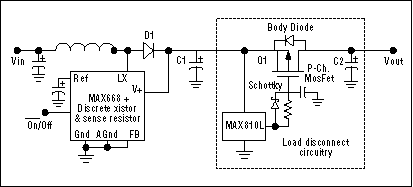
Figure 3. Adding three components in the MOSFET-gate circuit of Figure 2 provides the slow-connect/fast-disconnect necessary to accommodate heavy startup loads.
These circuits require a logic-level p-channel MOSFET such as Q1 to fully enhance the channel and obtain a low Rds-on. If Q1's on-resistance is high enough to cause a significant voltage drop (especially in low-output-voltage applications, or if the load is relatively far away), then it can be desirable to regulate the drain side of Q1. In doing this, you should minimize parasitics and observe good circuit-layout techniques. This remote regulation can be implemented with a SPDT, low-voltage analog switch in a SOT23 package (MAX4544), controlled by the MAX810's output state (Figure 4).
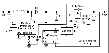
Figure 4. Further embellishments (to Figure 3) add remote-sense regulation and low-voltage detection to the boost converter with load disconnect.
The MAX4544 operates within data-sheet limits for supply voltages as low as 2.7V. With the input supply at 3.3V and about 0.3V across the Schottky diode, the MAX4544 (and MAX810) remains operational even when the boost converter is shut down. The MAX810 output is high during shutdown, connecting the MAX4544 COM node to NO (the Q1 source). When the boost converter turns on, resistors connected to the MAX4544 COM pin provide feedback to the MAX668. MAX4544 on-resistance is 60Ω maximum with a 5V supply, so the feedback-resistor values should be much larger than that to minimize output-voltage errors. On-resistance is only 120Ω at 3V; thus, the MAX4544 switch errors are minimal even for lower output voltages.
When the boost circuit is enabled and after the timeout period has elapsed, the MAX810 output goes low and connects the load by means of Q1. Simultaneously, the MAX810 output also causes the feedback resistors to switch over to the drain side of Q1, thus allowing output-voltage regulation at the load, which is remote to the main boost circuit.
This action also switches the MAX810 input to the drain side of Q1, where it can monitor overload conditions at the load. The foregoing arrangement is especially valuable if Q1's Rds-on causes a voltage drop greater than ~1% at the maximum load current. This can happen if Rds-on > 50mΩ at > 1A output on a 5V supply.
In response to a current overload, the MAX810 output goes high and quickly turns off Q1 through the Schottky diode. Simultaneously, it switches itself and the feedback resistors back to the source (input) side of Q1. The preceding configuration gives the boost output a chance to get back into regulation, after which the MAX810 reconnects the load. This cycle repeats until the overload is removed.
The MAX4544's break-before-make switching action is rather quick (10ns), so a small capacitor across the feedback resistors maintains the output voltage during the break period, to avoid disrupting the MAX668 feedback loop and to provide power to the MAX810. To prevent appreciable effects on the MAX668 transient response, this capacitor should be large enough to avoid significant discharge during the break period yet small enough to ensure a small time constant with the MAX4544 on-resistances.
The MAX4544's switch-control input has no Schmitt trigger, but it can tolerate slowly moving logic-level signals (these signals can, however, cause a 10-4A order of current to flow during the transition from the supply node to ground). The actual switch action is quick once the switching threshold is reached.
When using the MAX669 to boost low output voltages of 2.5V and below, a negative voltage may be required to fully enhance Q1. For example, an inexpensive, discrete charge pump attached to the LX node can generate -Vout + Vd (Figure 5). For a 2.7V output, it produces -2.0V with a standard pn-junction diode or -2.4V with a Schottky diode. This voltage is present whenever the boost converter is enabled, and it provides both a negative supply for the MAX4544 (which tolerates supply voltages to 12V) and biasing for Q1.
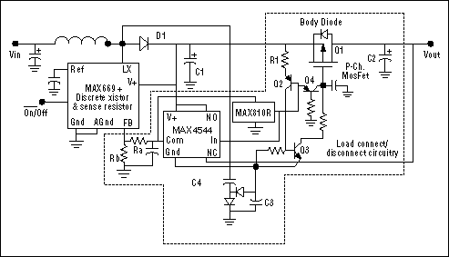
Figure 5. To achieve the load disconnect for low output voltages, this circuit ensures adequate drive to the MOSFET by generating a negative rail for the gate-drive IC (MAX810L).
Although Q1 turns on when the MAX810 output goes low, the MAX810's reset threshold cannot accurately sense the main output voltage with its ground terminal referred to the negative charge-pump output. Accordingly, the MAX810 ground terminal connects to ground and its output drives a level shifter comprised of Q2 and Q3, such that Q1's gate is pulled to the negative rail for turn-on.
The MAX668 features Idle Mode™ pulse frequency modulation (PFM) at light loads, which allows it to skip charging pulses when load current from the main supply is low. When pulses are skipped, Q2's emitter current (set by R1) discharges C3. This action can result in insufficient supply voltage to the MAX4544, even with the main output voltage in regulation. In turn, this effect can cause the on-resistance to skyrocket in the internal analog switch and the feedback voltage at the MAX668 to drop toward ground.
The MAX668 then tries to compensate by raising its output voltage, possibly resulting in an overvoltage condition. As an antidote, make sure the feedback resistors (the minimum DC load on the main output voltage) are small enough to discharge Vout slightly faster than the discharge of C3 by Q2's emitter current. Whether Q1 conducts or not, the following inequality lets you size C3:
C4 can be small compared to C3 if no charging pulses are skipped during normal PWM operation; but the more pulses are skipped, the larger C4 has to be. When boosting action resumes after pulse skipping, while Q2 is held off, C4 should be large enough to charge C3 before C1 becomes charged fully.
(Vout-Vbe)/(R1 × C3) < Vout/[(Ra+Rb)×(C1+C2)].
Many components and interconnects affect the MAX668 feedback path shown in Figures 3 and 4, and a fault in these components can produce an overvoltage Vout that destroys the load. For added safety, a zener diode (not shown) connected from C1 to the MAX668 FB pin (with its anode connected to FB) can provide an overriding local feedback loop that clamps the output at (Vz + VFB). To prevent a large overvoltage, set Vz equal to the maximum regulated Vout minus the maximum VFB.
If the system must control multiple loads individually while the boost converter remains on, you can replace the MAX810 with a MAX812 (in a 4-pin SOT143 package). The MAX812's fourth pin is designed for manual-reset applications, but it can force a disconnect between the local load and main boosted output by acting as a logic-level signal that overrides each smart solid-state fuse. This approach lets you control each load on the main boost supply independently.
Last but not least, this smart solid-state fusing technique, which auto-resets without power cycling and requires no replacement or field troubleshooting, need not be limited to boost-converter outputs. It can replace a fuse on the DC-power bus of virtually any system, regardless of voltage. (Bus voltages higher than 60V can require non-logic-level FETS and level shifters for the MAX810 output.) Using just two precision resistors to set an appropriate external bias for the higher voltages (Figure 6), you can set the solid-state fuse to be triggered by a programmed sag in the bus supply voltage.
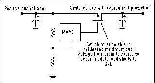
Figure 6. Extending the load-disconnect idea to non-boost-converter circuits forms a solid-state fuse that is applicable to any DC-power bus.
Suppose, for example, that -48 volts are to be protected against overcurrent. We interrupt the rail side instead of the ground side, because the voltage source is negative and we use an n-channel FET plus a MAX809T reset circuit, whose reset-output polarity is opposite to that of the MAX810. The supply voltage can range down to -36V under normal operation (Figure 7).
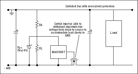
Figure 7. This solid-state fuse protects a negative DC-power bus.
Design equations are as follows:
The MAX809 quiescent current is about 100µA maximum over temperature, and the current through Rh and RL should be about 100 times' higher to minimize the effect of quiescent current on trip voltage: 36/(Rh+RL) = 10 mA, therefore
The MAX809 threshold is much lower than the supply-trip voltage, so RL is smaller than Rh, approximately by the ratio Vthreshold/(Vthreshold + Vsupply-trip) = 3/(36+3) = 0.077. Thus, MAX809 Iq flows through ~93.3% of (Rh+RL), causing a voltage-trip contribution of ~0.336V. Taking this fact into account, set the initial trip voltage for calculating Rh and RL at 36V - 0.336V = 35.664V. Using 1% resistors for Rh and RL, Vsupply-trip = 35.664V. This threshold occurs when the MAX809T threshold is at its minimum (3.15V, over the temperature range -40°C to + 85°C):
(Rh+RL) = 3600 Ohms.
Calculated values for RL and Rh are 323.81Ω and 3276.19Ω, respectively. The closest 1% values are 320 and 3280. Considering these resistor values and the 100µA Iq, the maximum supply-trip voltage becomes 36.09V, which surpasses 36V slightly. This result also occurs only for simultaneous worst-case values for all errors, which are rare scenarios in practice. For most applications, the foregoing design would be quite acceptable. The MAX809's nominal threshold voltage gives a nominal trip voltage of -34.65V.
35.664V[RL(0.99)/(RL(0.99)+Rh(1.01))] = 3.15V.
Rh should have a power rating of 0.5W. Because the voltage across RL exceeds the MAX809's maximum input-voltage rating when Vsupply goes above its minimum limit, place a 5V ±5% zener diode across RL as shown.
欢迎分享,转载请注明来源:内存溢出

 微信扫一扫
微信扫一扫
 支付宝扫一扫
评论列表(0条)