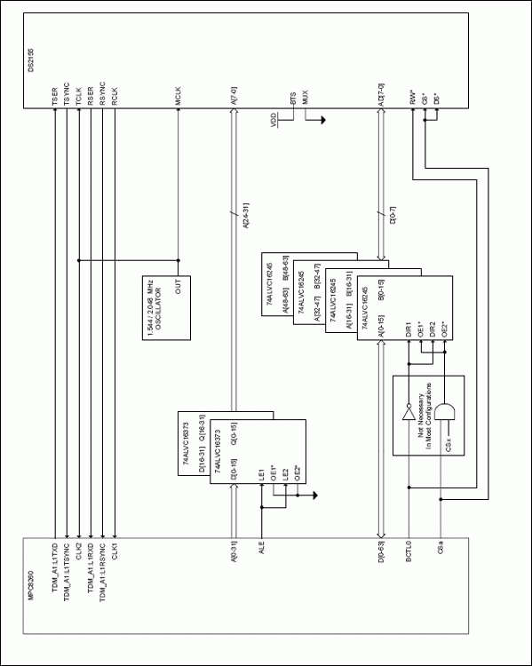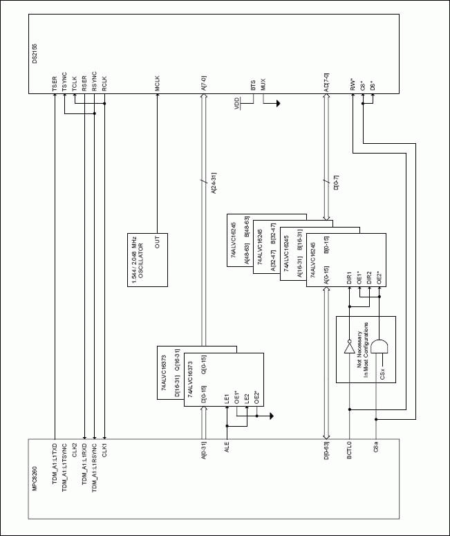
Interfacing the DS2155 to the Motorola MPC8260 PowerQUICC II can be accomplished many ways, depending on the intended application. The diagram in Figure 1 shows how the DS2155 is used as the master timing source in the T1/E1 system. The oscillator is connected to the master clock (MCLK) as well as the transmit clock (TCLK). Therefore, the DS2155 sources the clock and data signal to other T1/E1 devices. The diagram in Figure 2 shows how the DS2155 is used in a loop-timed T1/E1 system. The oscillator is connected to the master clock (MCLK) while the recovered clock (RCLK) is connected to the transmit clock (TCLK). In this design, the DS2155 receive and transmit clocks are locked.
The local bus interface in these two diagrams is identical. Although there is a dedicated local bus on the MPC8260, the pins of this bus are shared with the PCI interface pins. Because of this, the choice was made to connect the DS2155 off of the MPC8260 60x bus with minimal interface circuitry. For the 32-bit address bus, two 74ALVC16373 16-bit latch devices are connected to isolate the peripherals from the 60x bus. On the 64-bit data bus, four 74ALVC16245 16-bit transceiver devices are connected to isolate the peripherals from the 60x bus. Depending on the complexity and number of peripherals that are connected in this fashion to the 60x, the extra inverter and the AND gate for the data bus might not be necessary. The BCTL0 line can be configured for RD/WR* or RD*/WR, which may eliminate the need for the inverter depending on the peripherals that are connected. Also, if the peripheral address space is contiguous, the AND gate could be replaced by one of the 12 chip-select lines on the MPC8260. It is also important to note the reversing of the address and data lines of the MPC8260. The DS2155 address lines A[7–0] map to the 60x bus address lines A[24–31]. Likewise, the DS2155 data lines AD[7–0] map to the 60x bus data lines D[0–7]. In addition, if no other peripherals are connected to the 60x bus, it is possible to reduce both the number and bit size of the latch and transceiver devices since the DS2155 is only an 8- bit device.
The MPC8260 has two separate serial interface (SI1 and SI2) blocks, each of which has a time-slot assigner (TSA) that supports four time-division-multiplexed (TDM) channels. The four TDM channels for SI1 are referred to as TDMa1, TDMb1, TDMc1, and TDMd1. All of the associated signals and physical pins for SI1 are described in Table 1. The four TDM channels for SI2 are referred to as TDMa2, TDMb2, TDMc2, and TDMd2 (Table 2). For flexibility, each TDM channel can have a separate transmit and receive clock. The source of both the transmit and receive clock can be from two different clock inputs. Table 3 contains all eight TDM channels and the two possible clock sources for the transmit and receive channel.
To simplify the circuits in Figure 1 and Figure 2, TDMa1 was chosen at the transmit and receive path for the DS2155 data. A system that incorporated up to eight DS2155s could be easily obtained by using all eight TDM channels from the two SI blocks. For more information about the operation of the TSA in the MPC8260, see the MPC8260 PowerQUICC II User’s Manual. Chapter 14 of the user manual contains information about how to configure each TDM channel and how the data is stored in memory.

Figure 1. DS2155 Master Timing Source.

Figure 2. DS2155 Loop Timed.
Table 1. MPC8260 Serial Interface 1
TDM_B1:L1TXD
TDM_C1:L1TXD
TDM_D1:L1TXD PA9
PD13
PB15/PD28
PB11/PD25 Transmit data output for the serial interface TDM channel.
TDM_B1:L1RXD
TDM_C1:L1RXD
TDM_D1:L1RXD PA8
PD12
PB14/PD27
PB10/PD24 Receive data input for the serial interface TDM channel.
TDM_B1:L1TSYNC/GRANT
TDM_C1:L1TSYNC/GRANT
TDM_D1:L1TSYNC/GRANT PA7
PD11
PB13/PD16
PB9/PD4 Transmit data sync signal for the serial interface TDM channel.
TDM_B1:L1RSYNC
TDM_C1:L1RSYNC
TDM_D1:L1RSYNC PA6
PD10
PB12/PD26
PB8/PD23 Receive data sync signal for the serial interface TDM channel.
TDM_B1:L1RQ
TDM_C1:L1RQ
TDM_D1:L1RQ PB17
PB13
PC7
PC13 D-channel request signal for the serial interface TDM channel.
TDM_B1:L1CLKO
TDM_C1:L1CLKO
TDM_D1:L1CLKO PB16
PB12
PC6
PC11 Clock output from the serial interface TDM channel.
SI1:L1ST2
SI1:L1ST3
SI1:L1ST4 PC9
PC8
PC12
PC10 Four output strobes that can be generated by the serial interface.
Table 2. MPC8260 Serial Interface 2
TDM_B2:L1TXD
TDM_C2:L1TXD
TDM_D2:L1TXD PA9
PD13
PB15/PD28
PB11/PD25 Transmit data output for the serial interface TDM channel.
TDM_B2:L1RXD
TDM_C2:L1RXD
TDM_D2:L1RXD PA8
PD12
PB14/PD27
PB10/PD24 Receive data input for the serial interface TDM channel.
TDM_B2:L1TSYNC/GRANT
TDM_C2:L1TSYNC/GRANT
TDM_D2:L1TSYNC/GRANT PA7
PD11
PB13/PD16
PB9/PD4 Transmit data sync signal for the serial interface TDM channel.
TDM_B2:L1RSYNC
TDM_C2:L1RSYNC
TDM_D2:L1RSYNC PA6
PD10
PB12/PD26
PB8/PD23 Receive data sync signal for the serial interface TDM channel.
TDM_B2:L1RQ
TDM_C2:L1RQ
TDM_D2:L1RQ PB17
PB13
PC7
PC13 D-channel request signal for the serial interface TDM channel.
TDM_B2:L1CLKO
TDM_C2:L1CLKO
TDM_D2:L1CLKO PB16
PB12
PC6
PC11 Clock output from the serial interface TDM channel.
SI2:L1ST2
SI2:L1ST3
SI2:L1ST4 PC9
PC8
PC12
PC10 Four output strobes that can be generated by the serial interface.
Table 3. MPC8260 Serial Interface Clock Matrix
欢迎分享,转载请注明来源:内存溢出

 微信扫一扫
微信扫一扫
 支付宝扫一扫
评论列表(0条)