The DS2141A, DS2143, DS2151 and DS2153 contain some internal circuitry to allow them to more easily interface to an external controller that has a non-multiplexed address/data bus. In multiplexed schemes like the DS2141A, DS2143, DS2151 and DS2153 uses, a signal exists (usually called Address Strobe or Address Latch Enable) to denote that a valid address is present on the bus. This signal is necessary because the address and data lines share the same bus. In non-multiplexed schemes, this signal may not be supplied by the controller because the address and data lines are separated. The DS2141A, DS2143, DS2151 and DS2153 contains some onboard circuitry that enables it to internally create an address latch if it is used on a non-multiplexed bus.
The creation of this internal address latch occurs as follows. In the Intel timing set, when the ALE pin on the DS2141A, DS2143, DS2151 and DS2153 is high, if the WR pin goes active (i.e., low), then the address will be latched on the rising edge of WR. In the Motorola timing set, when the AS pin is high and the R/W pin is low, if the DS pin goes active (i.e., high), then the address will be latched on the falling edge of DS.
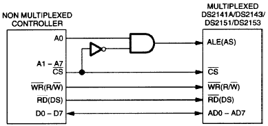
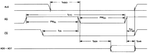
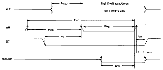
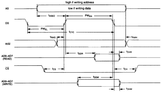
As an example, in a non-multiplexed system, A0 could be tied to the ALE (or AS) input. Please see Figure 1. Each read or write to the DS2141A, DS2143, DS2151 and DS2153 would consist of two operations. To write to the DS2141A, DS2143, DS2151 and DS2153, first the controller would write the address and then the data. To read from the DS2141A, DS2143, DS2151 and DS2153, the controller would first write the address and then read the data. The addresses would be treated as data by the controller. The addresses would reside in odd numbered bytes while the data would reside in even numbered bytes. Please see Figures 2 through 4 for timing information. The parametrics listed in the DS2141A, DS2143, DS2151 and DS2153 data sheets are valid for non-multiplexed bus operation as well.

Figure 1. Non-multiplexed bus configuration.

Figure 2. Non-multiplexed intel read timing.

Figure 3. Non-multiplexed intel write timing.

Figure 4. Non-multiplexed motorola timing.
欢迎分享,转载请注明来源:内存溢出

 微信扫一扫
微信扫一扫
 支付宝扫一扫
评论列表(0条)