The 24Cxx series of 2-wire serial EEPROMs are widely used in 8051 microprocessor systems. Although the MAX7651/MAX7652 flash-programmable 12-bit data acquisition systems have 16K of internal flash memory, there are many "legacy" products that use small and inexpensive external memories.
This application note provides basic 2-wire WRITE and READ software subroutines. They can be easily modified to address additional features of EEPROMs, such as memory protection and bank addressing.
There are many derivatives of the 24C02 serial EEPROM, which include additional memory and page addressing. The 24C02 is widely used and is the part used in this example. Other derivative parts can use this code with minor modifications. EEPROM Signals and Timing
The SDA signal is bi-directional, and is physically an open-drain so that multiple EEPROMs or other devices can share the pin. Both SCL and SDA must be pulled high externally.
The protocol used by the EEPROM is based in part on an ACK (acknowledge) bit sent by the EEPROM, if the data sent to it has been received. All addresses and data are sent in 8-bit words. The EEPROM sends the ACK as a low bit period during the ninth clock cycle. The EEPROM looks for specific transitions on the SCL and SDA pins to qualify READ and WRITE.
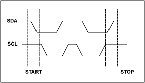
Data on the SDA pin may change only during the time SCL is low. Data changes during SCL high periods indicate a START or STOP condition. A START condition is a high-to-low transition of SDA with SCL high. All data transfers must begin with a START condition.
A STOP condition is a low-to-high transition of SDA with SCL high. All data transfers must end with a STOP condition. After a READ, the STOP places the EEPROM in a standby power mode. Refer to Figure 1 for START and STOP conditions.

Figure 1. START and STOP conditions. Device AddressingThe 24C02 has 3 physical pins, designated A2, A1, and A0, which are tied to logic 1 or 0 levels. This allows eight unique hardware addresses, so that up to eight 24C02s can share the SCL and SDA lines without conflict. There is an internal address comparator that looks for a match between the address sent by the master controller and the 24C02's unique 7-bit address, determined in part by A2, A1, and A0. Refer to Table 1below.
Table 1. 24C02 Device Address
欢迎分享,转载请注明来源:内存溢出
赞
(0)
打赏
 微信扫一扫
微信扫一扫
 支付宝扫一扫
 微信扫一扫
微信扫一扫
 支付宝扫一扫
采用MAXQ1850评估套件(EV kit)和面向MAXQ3
上一篇
2022-08-05
微控制器的设计指引进修信号噪声降低-Microcontrol
下一篇
2022-08-05

评论列表(0条)