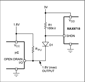
Typical peripheral CMOS I/O pins have a VIH of (0.7 x VDD) and a VIL of (0.3 x VDD). When powered from a 3V supply, these voltages are 2.1V and 900mV, respecTIvely. Valid digital signals connected to these logic pins must drive higher than VIH, and pull lower than VIL, to ensure proper communicaTIon. The circuit in Figure 1 shows the MAX9718, a 1.4W audio power amplifier that employs a CMOS acTIve-low SHDN input. The VIH and VIL levels of the active-low SHDN input are as described above.
The µC I/O in Figure 1 is an open-drain I/O pulled up to 1.8V. When the open-drain output is low, the voltage at the MAX9718's active-low SHDN pin is equal to one diode-forward voltage above GND, about 0.7V, which is well below the VIL of the MAX9718's active-low SHDN input. When the open-drain output goes high, the voltage at active-low SHDN rises to 2.5V and the MAX9718 is able to turn on.

Figure 1. Simple level translator.
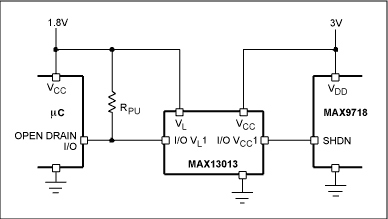
Integrated level translators are available to simplify interconnect between two devices that do not share the same power supply. Devices such as the MAX13013 can translate a 1.2V digital signal to a 3.6V device at a speed of 100Mbps. Figure 2 shows the proper connections for using the MAX13013 to interface a µC with the MAX9718.

Figure 2. Using the MAX13013 to interface a µC to the MAX9718.
欢迎分享,转载请注明来源:内存溢出

 微信扫一扫
微信扫一扫
 支付宝扫一扫
评论列表(0条)