
Using a UART to Implement a 1-Wire Bus Master
Abstract: This applicaTIon note explains how to use a microprocessor's UART to implement a 1-Wire® bus master. It includes an explanaTIon of the required electrical interface, UART configuraTIon, and TIming relationship between UART and 1-Wire signals. The flexibility offered in setting up UART byte timing allows straightforward implementation of 1-Wire time slots as well as the reset and presence detect pulses. With the inclusion of deep transmit and receive FIFOs, several byte values can be transferred on the 1-Wire bus with just a few clock cycles per bit required from the main processor.
1-Wire devices provide economical solutions for identification, memory, time keeping, measurement and control. The 1-Wire data interface is reduced to the absolute minimum, i.e., a single data line plus a ground reference. As most 1-Wire devices provide relatively small amounts of data, the typical data rate of 16kbps is more than sufficient for the intended tasks. It is often convenient to use a generalpurpose input/output (GPIO) pin of an 8-bit or 16-bit microcontroller in a "bit banging" manner to act as the bus master.
However, in 32-bit systems, processor clock frequencies routinely exceed 100MHz and using a GPIO pin as the 1-Wire bus master consumes an enormous number of clock cycles per 1-Wire bit. In 32-bit portable systems, precious battery power is consumed while timing the 1-Wire read- and write-time slots. A few systems off load the burden of bit timing and byte framing operations from the main processor by including the DS1WM Synthesizable 1-Wire Bus Master* hardware block in their chipset. If the DS1WM or other hardware 1-Wire master port is not available, communication with 1-Wire devices can be accomplished easily if a Universal Asynchronous Receiver Transmitter (UART) channel is available.
This application note includes an explanation of the required electrical interface, UART configuration, and timing relationship between UART and 1-Wire signals. A general understanding of 1-Wire communications is assumed. Typical timing and logic levels are used in the following discussion and the reader should refer to particular 1-Wire device data sheets for specific timing and voltage specifications and tolerances.
Properly configured with respect to baud rate, data bits per character, parity and number of stop bits, a 115,200 bit per second capable UART provides the input and output timing necessary to implement a 1-Wire master. The UART produces the 1-Wire reset pulse, as well as read- and write-time slots. The microprocessor simply puts one-byte character codes into the UART transmit register to send a 1-Wire 1 or 0 bit and the UART does the work. Conversely, the microprocessor reads single-byte character codes corresponding to a 1 or 0 bit read from a 1-Wire slave. All 1-Wire bit transfers require the bus master, the UART, to begin the cycle by driving the 1-Wire bus low. Therefore, each 1-Wire bit cycle includes a byte transmit and byte receive by the UART. When reading, the received data is of interest, when writing, however, the receive byte is discarded. Depending on the UART's read and write firstin, first-out (FIFO) buffer depth, the UART can also frame 1-Wire bits into byte values further reducing the processor overhead.
UART to 1-Wire Electrical Interface1-Wire devices operate in an open-drain environment on bus voltages ranging from 2.0V to 5.5V. Exact logic levels and minimum pullup voltages are device dependent, though generally parasite-power devices require minimum pullup voltage of 2.8V to recharge an internal storage capacitor used to supply power during periods when the data line is low. A 4.7kΩ resistor typically serves as the pullup on the 1-Wire data line. The resistor provides logic-high signals passively, with the bus master and all slave devices driving the logic-low signals. Devices usually include a weak internal pulldown, shown as Ipd in Figure 1.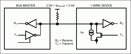
Figure 1. 1-Wire bus interface circuitry.
Since most UART transmit data (TXD) pins are not open drain, an external open-drain buffer circuit is usually needed. This circuit can be constructed out of discrete components as shown in Figure 2a, or integrated solutions such as the Fairchild NC7WZ07 shown in Figure 2b are available. In both circuits, the 4.7kΩ pullup resistor provides the logic high on the 1-Wire bus.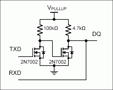
Figure 2a. Discrete open-drain buffer.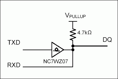
Figure 2b. Integrated open-drain buffer.
The timing diagrams in Figures 4 through 8 describe the relationship between 1-Wire time slots and UART byte frames. The reader is reminded that the UART serves as the bus master, and therefore begins all bit transfers on a high to low transition of the TXD output. Since the electrical interface ties the buffered TXD signal to receive data (RXD) input pin, the UART receives a byte for every byte transmitted. The operation is similar to loop-back testing.
Each diagram includes a UART configuration, transmit byte value and expected receive byte value. The listed UART configurations produce waveforms compliant with regular mode 1-Wire timings. Note that the UART is configured with a different baud rate for the reset and presence detect than with the read- and write-time slots. It is possible to use other configurations as well, although the evaluation criteria can be different from those shown in the timing diagrams. The transmit byte value corresponds to the 1-Wire bus master role, and the receive byte value or range represents the expected activity on the bus. When reading, the receive value needs to be evaluated to determine the bit value returned by the 1-Wire slave device. The read 0 and read 1 evaluation criteria are included in the diagrams. The read-back value or range of values to determine a successful presence detect is also included. The Timing Diagram Legend applies to the timing diagrams in Figures 4 through 8, and explains the graphical nomenclature of illustrated 1-Wire bus activity.
Figure 3. Timing diagram legend.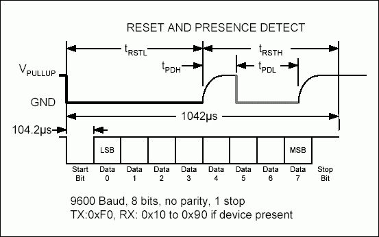
Figure 4. Reset pulse and presence detect.
In Figure 4, generation of the Reset pulse and detection of the Presence pulse returned by any 1-Wire devices on the bus use a baud rate of 9600. Transmitting an 0xF0 from the UART forms a proper Reset pulse. The receive value depends on whether one or more 1-Wire slave devices are present, their internal timing of each slave device present, and the UART's detection timing within each bit window. If no device is present, the receive value will equal the transmit value. Otherwise the receive value can vary. A single slave device running at minimum internal timing will change the response to 0xE0. A single slave running at maximum internal timing will change the response to 0x90. 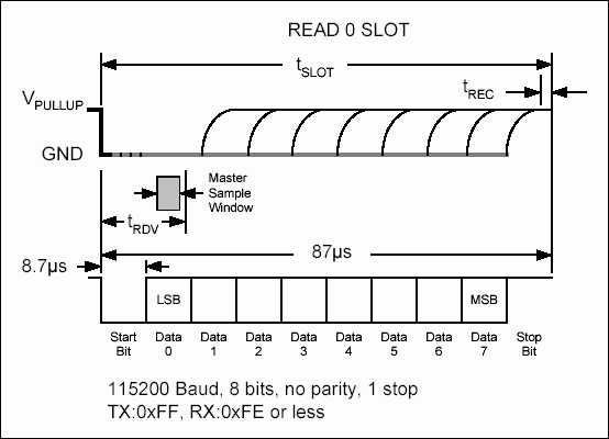
Figure 5. Read 0 time slot.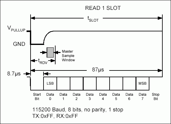
Figure 6. Read 1 time slot.
Read and Write Time Slots generated in Figures 5-8 use a baud rate of 115,200. The receive value from a read 0 will range from 0xFE to 0x00 depending on the internal timebase of the 1-Wire slave device. In order to transmit a 1-Wire 0 bit value, the 1-Wire slave must hold the data line low for tRDV which extends through the LSB bit period for the given UART configuration. The receive value from a read 1 will always be 0xFF, since the 1-Wire slave allows the data line to return to a 1 state as soon as the bus master releases it. Once the receive byte is retrieved from the UART, the LSB should be tested to determine if the slave returned a read 0 or a read 1.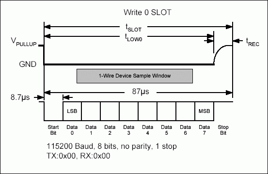
Figure 7. Write 0 time slot.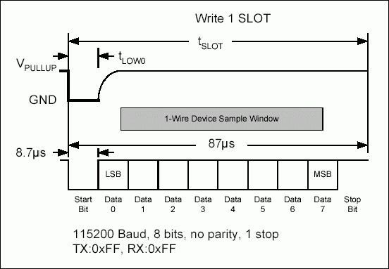
Figure 8. Write 1 time slot.
Write time slots do not require evaluation of the receive value, since the 1-Wire slave does not assert a low on the data line. The read-back values for write 0 and write 1 are provided for convenience only, though the write 1 receive value could be used to detect a stuck low fault on the bus. The receive register or FIFO must be read or cleared during the write operation on most UARTs.
A key advantage to the 1-Wire bus is the flexibility in bit-to-bit timing. The delay between bits can be as short as tREC minimum, or as long as the bus master deems necessary. There is no maximum delay period between 1-Wire bits or bytes. Therefore, the processor can service the UART at its leisure in framing bit time slots into byte values. Communication with 1-Wire devices can be designated as a low-priority task. The processor need not waste processing cycles or power, or neglect high-priority time-critical tasks.
Figure 9. Bit-to-Bit timing flexibility.
Processors with deep FIFOs on the transmit and receive channels can further decrease processor overhead by queuing several bits at a time. The following table shows the FIFO depth for several popular 32-bit microprocessors, and the number of 1-Wire bits that can be sent or received at a time.
On the Intel PXA250, the entire 64-bit ROM ID or 8 byte wide registers can be read in by clearing the receive FIFO, filling the transmit FIFO with 0xFF with the FIFO mode enabled. The receive FIFO fills with the data returned by the 1-Wire slave device. Using DMA channels can increase the autonomous operation of reading or writing blocks of data larger than the FIFO depth. Conclusion
The venerable UART remains a valuable peripheral on modern processors because of its programmability. The flexibility offered in setting up UART byte timing allows straightforward implementation of 1-Wire time slots as well as the reset and presence detect pulses. With the inclusion of deep transmit and receive FIFOs, several byte values can be transferred on the 1-Wire bus with just a few clock cycles per bit required from the main processor.
1-Wire is a registered trademark of Maxim Integrated Products, Inc.
DragonBall is a trademark of Motorola, Inc.
Intel XScale is a registered trademark of Intel Corporation.
欢迎分享,转载请注明来源:内存溢出

 微信扫一扫
微信扫一扫
 支付宝扫一扫
评论列表(0条)